The Superconducting Circuit Board

    Omni Team

    Find me on:

    Recent Posts

    Understanding Printed Circuit Board Manufacturing: Multilayer Assembly

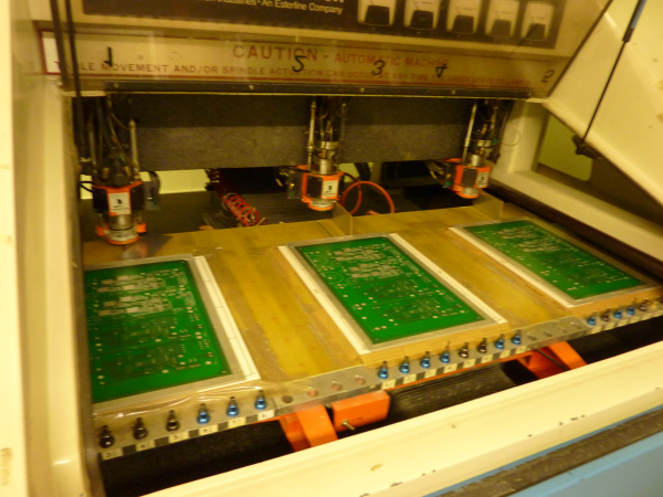
    One of the more interesting activities routinely associated with PCB manufacturing is the process of assembling multilayer circuit boards.

    At any given time 60% of our PCB manufacturing at Omni is producing multilayer circuit boards, so understanding the process is important. Layers of copper foil, pre-preg and core material are sandwiched together under high temperature and pressure to produce multilayer assemblies. Pressure is needed to squeeze out air while heat is required to melt and cure the thermosetting “pre-preg” adhesive which holds the multilayer PCB together.

    Measuring and Calculating the Resistance of Aluminum Trace (very low temperature) Printed Circuit Boards

    Measuring resistance of a fine-line Aluminum Trace provides different challenges compared to traces on a Copper PCB, most importantly, the surface aluminum oxide is tenacious and it can be difficult to get through to arrive at an accurate and repeatable measurement.

    Development of Very Low Temperature Printed Circuit Boards (Aluminum Trace, Superconductive, Cryogenic PCBs)

    Mid 2011 was the beginning of the collaboration between Omni Circuit Boards and D-Wave Systems to produce superconducting, low temperature printed circuit boards (PCBs)

    Development was driven by D-Wave’s need for low temperature PCBs which could provide mono-metal superconductive connection to their unique quantum processors (QPUs).

    The PCBs would operate at cryogenic low-temperature, be solderable and be suitable for wire-bonding. The PCB would also withstand multiple temperature cycling from below 500 Millikelvin to 20°C.

    Understanding Printed Circuit Board Manufacturing: CNC Drilling

    One of the key processes in a PCB manufacturing facility is the CNC Drilling Department.

    Holes are drilled in PCBs for two main reasons:

    Customer requirements.- PTH component mounting and to promote conductivity between Cu layers (vias)

    Manufacturing requirements.- To ensure precise registration and to help the operator ensure each drill has successfully completed the tool path.

    Custom Printed Circuit Board Shapes

    In business as in life, we learn more from listening than talking.

    The other day we received a fairly odd question from an electrical engineer with a product development company we have worked with for many years.

    “Can you do round circuit boards?” he asked.
    “Yes…” we replied tentatively, thinking there must be so much more to the question.
    “So a board that’s three inches round… no problem?” he inquired.
    “Absolutely,” we confirmed.

    But then we began to think. If a long-time customer doesn’t know we have the capability to produce boards which aren’t just rectangular, how would a new customer know?

    4 Common Printed Circuit Board Design Mistakes to Avoid

    Avoid these four circuit board design mistakes:


    1.  Stipulating a "minus" tolerance on small micro via holes

    2.  Having Non-functional pads on inner layers

    3.  Not defining nor considering edge tolerances

    4.  Stipulating wrong copper thicknesses


    Understanding Printed Circuit Board Manufacturing: Working with Duroid laminates

    To begin, the laminate manufacturer freely admits the material will move, but only during the etching process.

    The key they state is to first etch 80% of the copper, cure the material in an oven, then provide a final etch and a final baking cure. 

    (Image by Jeff Keizer)

    When beginning work with a new material, you try to do as much research and get as much advice as possible.

    You download the manufacturers documentation and talk with the manufacturers representatives, drill/router bit manufacturers and other PCB manufacturers who have worked on the material in the past.

    After compiling all this information, a manufacturing process is developed which fits both the material and your own facility.


    Understanding Printed Circuit Board Manufacturing: Panelization

    The purpose of panelization is to secure PCB boards during manufacturing, shipping and assembly processes and faster throughput while making their separation as painless as possible.

    PCB Manufacturer = The company that manufactures blank PCBs for you, Omni Circuit Boards Ltd is a "PCB Manufacturer"

    PCBA Manufacturer = The company that manufactures an assembled or populated PCB for you, also known as CMs or contract manufacturers.


    How to Get a Low Cost Printed Circuit Board Quote

    We would like to offer you step by step instructions on how to get a PCB Quote.

    First the legal requirements: quotes form an integral part of the traditional, legal, offer and acceptance contract process.

    When you receive your quote, it is your responsibility to review the specifications provided.


    Quantum Computer Developer Chooses Omni as Superconductive Printed Circuit Board Manufacturer

    The technical expertise needed to build the world's first commercial quantum computer is immense.

    D-Wave Systems Inc. turned to Omni Circuit Boards to help them build the first "Superconductive Aluminum-Trace Printed Circuit Boards" that serves as interface with their QPUs (quantum processing units)