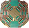
One of the more interesting activities routinely associated with PCB manufacturing is the process of assembling multilayer circuit boards.
At any given time 60% of our PCB manufacturing at Omni is producing multilayer circuit boards, so understanding the process is important. Layers of copper foil, pre-preg and core material are sandwiched together under high temperature and pressure to produce multilayer assemblies. Pressure is needed to squeeze out air while heat is required to melt and cure the thermosetting “pre-preg” adhesive which holds the multilayer PCB together.
How is a multilayer PCB manufactured?
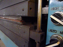
Manufacturing multilayer circuit boards is a straightforward process but does require a high level of attention to detail. Care must be taken to ensure all layers are correctly registered to the required drilled holes despite the deformation stresses produced by the heat and pressure. The buildup requires the operator ensures correct materials are chosen, the build sequence is followed and the orientation of each sheet is correct. Each unpressed PCB panel is loaded as a “chapter” with up to 10 chapters pressed together to form a “book” separated by heavy steel plates. These books are then loaded into each chamber of a hydraulic press. At Omni, we have the capacity to press up to 30 PCB panels in each load. The process for pressing polyimide material is modified slightly from the process required for FR4.
Specialized equipment for pressing multilayer
PCBs Manufacturing multilayer PCBs requires a specialized hydraulic press with heated platens. Initially the books are squeezed with a “kiss” pressure of 50 psi prior to being heated to 350F at 350 psi for a minimum of one hour. The assembly is then allowed to cool slowly before removal for further processing. At Omni, the maximum size of a multilayer board is 12”x 16” while the board thickness can range from 0.015”to 0.125”.
Design for Manufacturability (DFM) for multilayer circuit boards
- A few considerations will help ensure manufacturable PCB designs.
- Copper areas - on inner layers, all copper should be kept at least 10 mil from the outer edge of the board, 20 mil is preferred.
- Via clearance through inner layers (antipads)
- Allow for clearance around any holes or via barrels not connected to an inner layer. This clearance should be at least 15 mil although 20 mil clearance is preferred.
- Thermal Relief Pads - the tie should be a minimum of 8 mil while more is preferable.
- Larger geometries - will result in higher yields which will be reflected in your board price.
As an aid to multilayer board design, we are able to provide thickness specifications for some standard materials. All thicknesses are in mils (1 mil = 0.001 inch = 25.4 microns).
Multilayer Thickness Parameters
| Copper Foil (Outer Layers) | Approximate Thickness (mils) |
| 0.5 oz Cu foil | 0.67 |
| 1.0 oz Cu foil | 1.38 |
| 2.0 oz Cu foil | 2.76 |
| Electroplate (Outer Layers) | |
| 0.5 oz Cu | 0.67 |
| 0.7 oz Cu | 1.00 |
| 1.0 oz Cu foil | 1.38 |
| 1.5 oz Cu | 2.07 |
| 2.0 oz Cu foil | 2.76 |
| Prepreg Materials | |
| NP175FB 2116 (cured*) | 4.1 |
| NP175FB 7628MR (cured*) | 7.5 |
| Core Materials | |
| NP175FTL 0.005 H/H Cu | 6.2 |
| NP175FTL 0.010 H/H Cu | 10.8 |
| NP175FTL 0.010 1/1 Cu | 12.2 |
| NP175FTL 0.014 H/H Cu | 15.0 |
| NP175FTL 0.014 1/1 Cu | 16.4 |
| NP175FTL 0.021 1/1 Cu | 23.5 |
| NP175FTL 0.028 1/1 Cu | 30.5 |
*between solid foils (no void filling)
Bow and Twist in multilayer PCBs is typically the result of unconventional designs (Odd layer count PCBs).
Bow and twist is more likely to occur in asymmetric designs which can result in unbalanced stress conditions. For example, odd layer counts (3, 5 layer) are known to cause issues. Another source of multilayer PCB bow and twist comes from designs which specify variable layer thicknesses. For example, a 4 layer build specification of 7 / 28 / 21 creates more risk of deformation than a standard build. Even different circuit configurations can be influencing factors.
Final thickness standards for multilayer builds.
Final thickness varies somewhat depending on circuit patterns. Solid copper planes yield thicker boards than layers with little or no copper. Thickness tolerance is typically +/- 10%.
Multilayer Thickness Parameters
| Standard Multilayer Builds | Mils per Dielectric Layer | Resulting Thickness |
| 4 Layer | 14 / 28 / 14 | 62 mil |
| 6 Layer | 7 / 14 / 14 / 14 / 7 | 62 mil |
| 8 Layer | 7 / 5 / 11 / 5 / 11 / 5 / 7 | 62 mil |
| 10 Layer | 4 / 5 / 7 / 5 / 7 / 5 / 7 / 5 / 4 | 62 mil |
So how can understanding more about the PCB multilayer assembly process help you reduce your PCB costs?
Ensure the specifications you are requesting are truly needed. While deviations from standard “tried and true” recipes are often possible, each subtle change carries additional risk, usually reflected in higher pricing, slower delivery times and occasional failure which could require a re-design. Additionally, we strongly recommend electrical testing for most multilayer printed circuit boards. Today’s software has helped designers provide consistently more manufacturable PCBs and you should expect even better results when you infuse your designs with the considerations provided above.