The Superconducting Circuit Board

    Omni Team

    Find me on:

    Recent Posts

    Aluminum-Trace (very low temperature) Printed Circuit Board Innovation

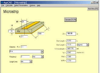
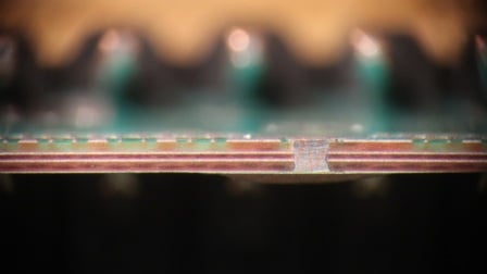
    The journey to develop a circuit board which features aluminum circuitry (Aluminum PCBs ) has been challenging.

    Beginning in 2008, Omni Circuit boards was challenged by a strategic partner with developing a circuit board with fine-line aluminum traces. The reason for aluminum in the initial quest was for its superconducting (cryogenic) properties. But as time went by, we began to appreciate how developing this capability could also benefit customers who have a requirement for aluminum wire bonding of critical components and non-magnetic properties.

    Understanding Printed Circuit Board Manufacturing: Odd Layer PCBs

    About 8% of PCB boards we are asked to produce are comprised of an odd number of layers. But unless you have a specific signal routing requirement or need for a greater dielectric space, it is usually best to design a multilayer board with an even number of layers. Reducing an even layered board by one layer may seem like a cost-saving move, but from a Printed Circuit Board perspective it is not. It may actually increase the cost as well as lead-time and leave you with a warped PCB which may not meet your expectations. Let's look at the issues in detail.

    Understanding Printed Circuit Board Manufacturing: Avoiding File Errors

    At Omni not all PCB files we receive are from seasoned PCB design professionals.

    Designs also come to us from enterprising individuals who can credit their body of knowledge to the results of internet searches. The inspiration for this article came from one such individual.

    How to Avoid Printed Circuit Board Delays in the Quoting Process

    CAM (computer-aided manufacturing) is the art of translating a PCB board designer’s creative CAD (computer-aided design) output into information required in the manufacturing processes required to fabricate that same PCB.

    Our processes require your computer generated files to be converted into photo-tooling films and drill and router files which will allow us, the printed circuit board manufacturing facility, to produce a custom PCB to your specifications.

    Understanding Printed Circuit Board Manufacturing: Hard Gold Plating

    Plating Hard Gold onto printed circuit boards is typically done to provide contact points and PCB edge connectors.

    Gold contact surfaces are often used on circuit boards with membrane switches which are a technology of choice for industrial, commercial and consumer products. When PCBs will be repeatedly installed and removed, electroplated gold is used for edge-connector contacts or as they are more commonly known: Gold fingers. The plating thickness of a PCB gold finger is typically a mere 300 micro-inch. At this thickness the hard gold is expected to survive 1,000 cycles before wear through.

    Printed Circuit Board Design Techniques and Best Practices for Cheaper Quotes

    Using a few simple techniques can help ensure a more robust printed circuit board design which can also help you save money.

    Printed circuit board design is a balance between functionality, longevity, aesthetics and board costs, time to design and the PCB fabricators capabilities. Listed below are eleven of the most common best practices we recommend to our customers.

    Understanding Printed Circuit Board Manufacturing: Silk-Screening

    One of the more artistic processes in a PCB manufacturing facility is the application of Silkscreen known in the old days as Ident layers.

    Silkscreen is usually white and human readable letters, normally used to identify components, test points, PCB and PCBA part numbers, warning symbols, company logos, date codes and manufacturer marks.

    Silk-screening requires specially formulated inks. The standard colour is white, but you can also select red, blue, black, yellow, etc.

    Understanding Printed Circuit Board Manufacturing: Impedance Control

    Printed circuit boards with impedance requirements demand a high level of precision.

    For standard circuit boards, a PCB manufacturer is given a set of patterns - copper patterns, hole patterns, ink patterns, which are combined into a single circuit board with all the pattern sizes and positions within certain tolerances. Failure to meet a certain size or position with the specified tolerance can be cause for the circuit board to be rejected. If a trace has been defined as an impedance control trace, it is not the trace size which is strictly defined, but rather the impedance. While a nominal trace size will be provided in the Gerber layer, it is understood the circuit board manufacturer can vary trace width, height, and dielectric thickness as long as the final impedance is within tolerance.

    How Copper Weight Impacts Printed Circuit Board Manufacturing - Copper Thickness Calculator

    One of the critical steps when ordering a printed circuit board is specifying the copper weight.

    The default, should you choose not to specify a weight, is 1.2 oz of copper. This is because customers routinely specify a minimum 1 oz copper thickness and 1 mil of copper in plated through holes. To achieve this, we routinely plate up 0.5 oz base material with 0.7 oz of additional copper which provides the requested thickness in the hole. Often our PCB board quotes will reflect this specifying 0.5 + 0.7 oz Cu/sq ft where the 0.5 is the base copper and the 0.7 is the plated copper.

    Why Omni Circuit Boards Ltd was the First Printed Circuit Board Manufacturer to Produce an Aluminum-Trace (very low temperature, superconductive, cryogenic) PCB

    Today's computing technology is rapidly outpacing the capabilities of standard, mass-produced printed circuit boards. 


    That's why it was no surprise when the engineers at British Columbia based D-Wave Systems came to us looking for a unique product.