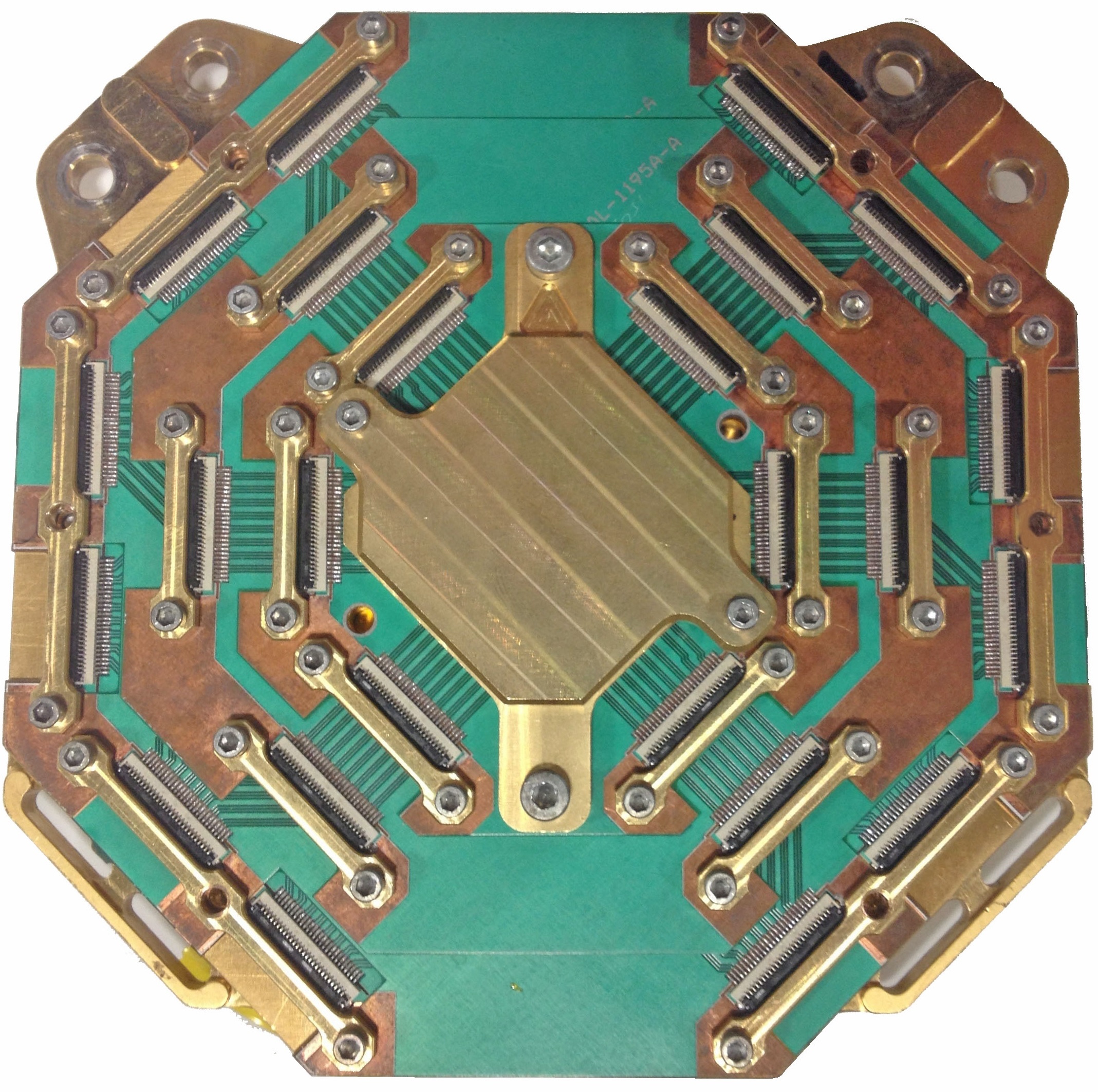

Tc = 1 Kelvin
0.005" minimum line/space
0.006" line/space for higher yield
≥ 0.008" for impedance controlled traces
Cryogenically tested
0.010" minimum pitch
0.012" pitch for higher yield
4 metal layers
Superconductive contact to inner layers
Two-tier bonding pads
Superconducting SMP connectors
Fully SC signal path (no copper)

OMNI produced the world's first etched aluminum/copper bimetal trace PCBs, opening the door for applications needing cryogenic temperatures, superconducting PCBs and chip interconnections using superconducting
OMNI also produces solderable aluminum trace PCBs suitable for aluminum-to-aluminum wire bonding that are used by R&D groups around the globe.

Leading-edge processes and PCBs call for more in-depth conversations. Contact our team at sales(at)omnicircuitboards.com.
We provide prototyping services for organizations that need answers, especially for cryogenic and superconducting applications.
1, 2, 4, 6 & 8 layer copper PCBs.
Specializing in ENIG & Immersion White Tin.
Scanned or layed-out from existing artwork or sample boards.