The problem when soldering to Aluminum
Aluminum reacts very quickly with oxidizers in the air. It immediately develops a passive layer of aluminum oxide surrounding the pure metal, making it difficult to solder than copper.
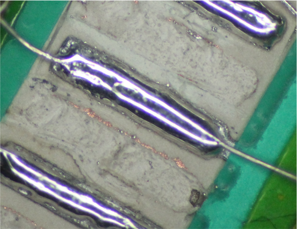
Aluminum reacts very quickly with oxidizers in the air. It immediately develops a passive layer of aluminum oxide surrounding the pure metal, making it difficult to solder than copper.
Fri, May 12, 2023 @ 02:51 PM Natalia Piedras Aluminum Trace PCB - Superconductive PCB
Read More »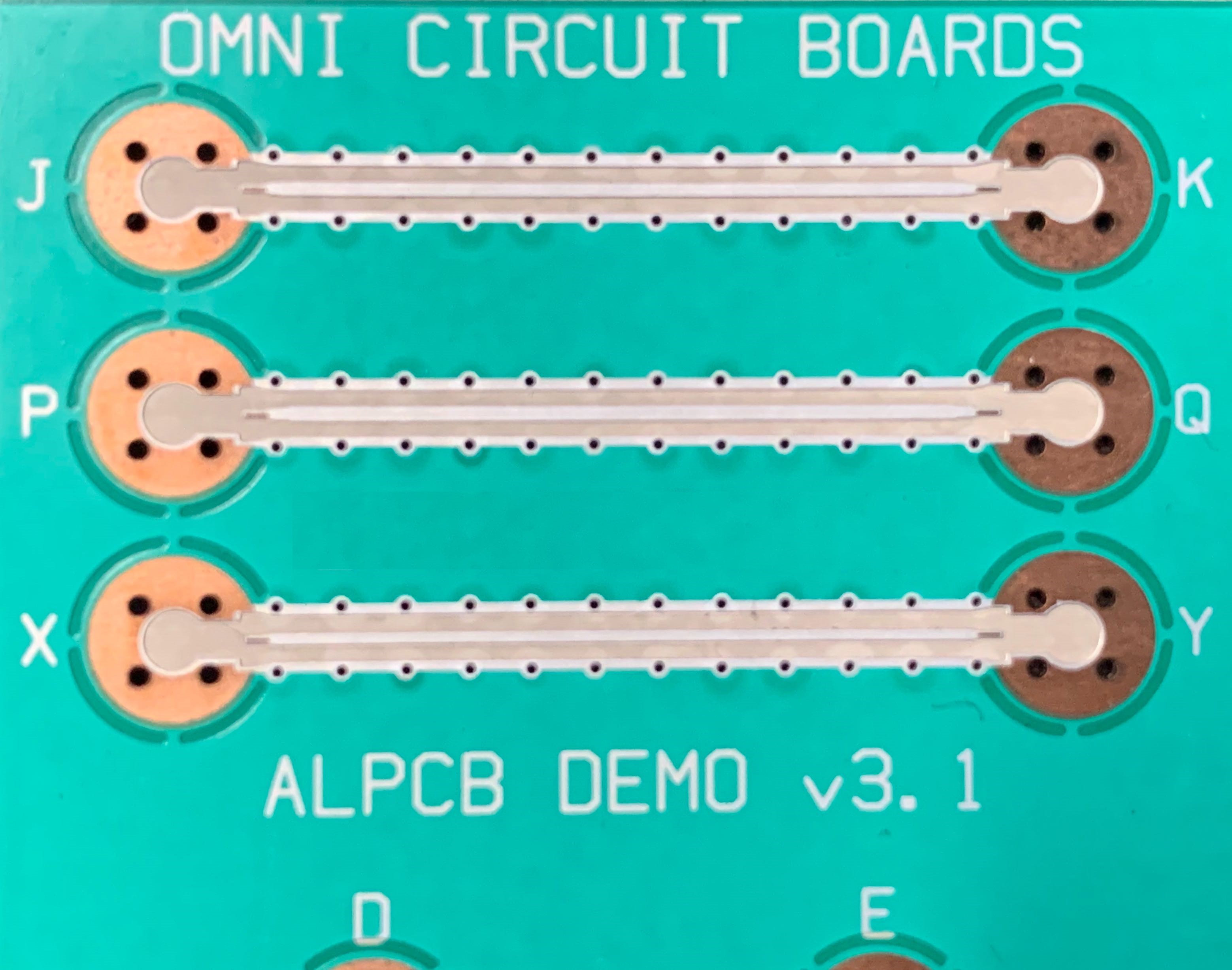
A circuit trace is a conducting track on a printed circuit board that connects components electrically and allows electric current to flow with little resistance.
While this small resistance is inconsequential for most applications, there are applications where the heat dissipated due to this small resistance is a big problem.
Much like how normal conducting trace allows current to flow, they also allow heat to flow from higher temperature areas to areas of lower temperature.
Mon, Jul 27, 2020 @ 01:11 PM Natalia Piedras Printed Circuit Board Design, Aluminum Trace PCB - Superconductive PCB
Read More »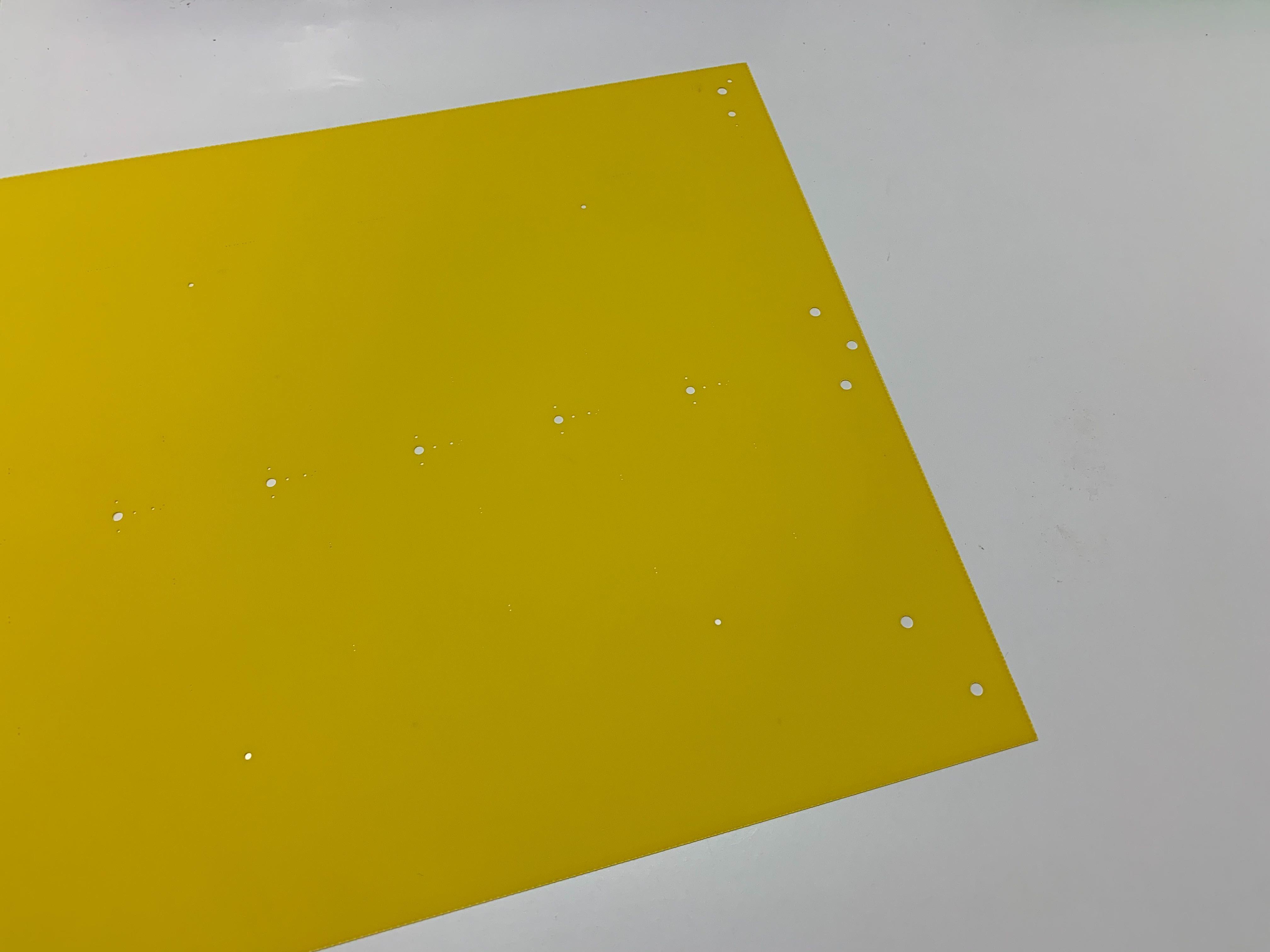
The short answer is "Yes," but there is a bit more to it.
What exactly is FR-4? FR-4 is a NEMA grade designation for flame-resistant glass-reinforced epoxy laminate. "FR" stands for Flame Retardant. The materials used are not defined by it, so different formulations can be rated FR-4. Unfortunately, it has become the norm in the industry to refer to the most commonly used PCB material by its FR-4 designation. As different formulations can share this rating, the properties of FR-4, particularly at cryogenic temperatures, can vary significantly.
Mon, Feb 03, 2020 @ 06:45 AM Natalia Piedras Printed Circuit Board Design, Printed Circuit Board Commentary
Read More »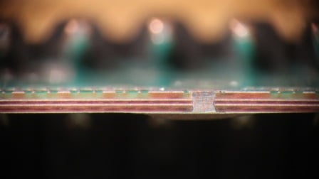
Beginning in 2008, Omni Circuit boards was challenged by a strategic partner with developing a circuit board with fine-line aluminum traces. The reason for aluminum in the initial quest was for its superconducting (cryogenic) properties. But as time went by, we began to appreciate how developing this capability could also benefit customers who have a requirement for aluminum wire bonding of critical components and non-magnetic properties.
Wed, Jan 22, 2020 @ 04:35 PM Omni Team Aluminum Trace PCB - Superconductive PCB
Read More »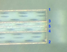
Mon, Dec 30, 2019 @ 11:55 AM Omni Team Printed Circuit Board Design
Read More »
Designs also come to us from enterprising individuals who can credit their body of knowledge to the results of internet searches. The inspiration for this article came from one such individual.
Mon, Dec 02, 2019 @ 01:48 PM Omni Team Printed Circuit Board Design
Read More »
Our processes require your computer generated files to be converted into photo-tooling films and drill and router files which will allow us, the printed circuit board manufacturing facility, to produce a custom PCB to your specifications.
Wed, Nov 27, 2019 @ 03:18 PM Omni Team Printed Circuit Board Design
Read More »
Gold contact surfaces are often used on circuit boards with membrane switches which are a technology of choice for industrial, commercial and consumer products. When PCBs will be repeatedly installed and removed, electroplated gold is used for edge-connector contacts or as they are more commonly known: Gold fingers. The plating thickness of a PCB gold finger is typically a mere 300 micro-inch. At this thickness the hard gold is expected to survive 1,000 cycles before wear through.
Fri, Nov 01, 2019 @ 03:47 PM Omni Team Printed Circuit Board Quote, Printed Circuit Board Design
Read More »
Printed circuit board design is a balance between functionality, longevity, aesthetics and board costs, time to design and the PCB fabricators capabilities. Listed below are eleven of the most common best practices we recommend to our customers.
Mon, Oct 28, 2019 @ 01:12 PM Omni Team Printed Circuit Board Design
Read More »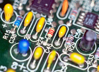
Silkscreen is usually white and human readable letters, normally used to identify components, test points, PCB and PCBA part numbers, warning symbols, company logos, date codes and manufacturer marks.
Silk-screening requires specially formulated inks. The standard colour is white, but you can also select red, blue, black, yellow, etc.
Thu, Oct 03, 2019 @ 04:08 PM Omni Team Printed Circuit Board Manufacturing
Read More »