The Superconducting Circuit Board

    Understanding Printed Circuit Board Manufacturing: Impedance Control

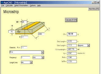
    Printed circuit boards with impedance requirements demand a high level of precision.

    For standard circuit boards, a PCB manufacturer is given a set of patterns - copper patterns, hole patterns, ink patterns, which are combined into a single circuit board with all the pattern sizes and positions within certain tolerances. Failure to meet a certain size or position with the specified tolerance can be cause for the circuit board to be rejected. If a trace has been defined as an impedance control trace, it is not the trace size which is strictly defined, but rather the impedance. While a nominal trace size will be provided in the Gerber layer, it is understood the circuit board manufacturer can vary trace width, height, and dielectric thickness as long as the final impedance is within tolerance.

    How Copper Weight Impacts Printed Circuit Board Manufacturing - Copper Thickness Calculator

    One of the critical steps when ordering a printed circuit board is specifying the copper weight.

    The default, should you choose not to specify a weight, is 1.2 oz of copper. This is because customers routinely specify a minimum 1 oz copper thickness and 1 mil of copper in plated through holes. To achieve this, we routinely plate up 0.5 oz base material with 0.7 oz of additional copper which provides the requested thickness in the hole. Often our PCB board quotes will reflect this specifying 0.5 + 0.7 oz Cu/sq ft where the 0.5 is the base copper and the 0.7 is the plated copper.

    Why Omni Circuit Boards Ltd was the First Printed Circuit Board Manufacturer to Produce an Aluminum-Trace (very low temperature, superconductive, cryogenic) PCB

    Today's computing technology is rapidly outpacing the capabilities of standard, mass-produced printed circuit boards. 


    That's why it was no surprise when the engineers at British Columbia based D-Wave Systems came to us looking for a unique product.

    Understanding Printed Circuit Board Manufacturing: Multilayer Assembly

    One of the more interesting activities routinely associated with PCB manufacturing is the process of assembling multilayer circuit boards.

    At any given time 60% of our PCB manufacturing at Omni is producing multilayer circuit boards, so understanding the process is important. Layers of copper foil, pre-preg and core material are sandwiched together under high temperature and pressure to produce multilayer assemblies. Pressure is needed to squeeze out air while heat is required to melt and cure the thermosetting “pre-preg” adhesive which holds the multilayer PCB together.

    Measuring and Calculating the Resistance of Aluminum Trace (very low temperature) Printed Circuit Boards

    Measuring resistance of a fine-line Aluminum Trace provides different challenges compared to traces on a Copper PCB, most importantly, the surface aluminum oxide is tenacious and it can be difficult to get through to arrive at an accurate and repeatable measurement.

    Development of Very Low Temperature Printed Circuit Boards (Aluminum Trace, Superconductive, Cryogenic PCBs)

    Mid 2011 was the beginning of the collaboration between Omni Circuit Boards and D-Wave Systems to produce superconducting, low temperature printed circuit boards (PCBs)

    Development was driven by D-Wave’s need for low temperature PCBs which could provide mono-metal superconductive connection to their unique quantum processors (QPUs).

    The PCBs would operate at cryogenic low-temperature, be solderable and be suitable for wire-bonding. The PCB would also withstand multiple temperature cycling from below 500 Millikelvin to 20°C.

    Understanding Printed Circuit Board Manufacturing: CNC Drilling

    One of the key processes in a PCB manufacturing facility is the CNC Drilling Department.

    Holes are drilled in PCBs for two main reasons:

    Customer requirements.- PTH component mounting and to promote conductivity between Cu layers (vias)

    Manufacturing requirements.- To ensure precise registration and to help the operator ensure each drill has successfully completed the tool path.

    Custom Printed Circuit Board Shapes

    In business as in life, we learn more from listening than talking.

    The other day we received a fairly odd question from an electrical engineer with a product development company we have worked with for many years.

    “Can you do round circuit boards?” he asked.
    “Yes…” we replied tentatively, thinking there must be so much more to the question.
    “So a board that’s three inches round… no problem?” he inquired.
    “Absolutely,” we confirmed.

    But then we began to think. If a long-time customer doesn’t know we have the capability to produce boards which aren’t just rectangular, how would a new customer know?

    4 Common Printed Circuit Board Design Mistakes to Avoid

    Avoid these four circuit board design mistakes:


    1.  Stipulating a "minus" tolerance on small micro via holes

    2.  Having Non-functional pads on inner layers

    3.  Not defining nor considering edge tolerances

    4.  Stipulating wrong copper thicknesses


    Understanding Printed Circuit Board Manufacturing: Working with Duroid laminates

    To begin, the laminate manufacturer freely admits the material will move, but only during the etching process.

    The key they state is to first etch 80% of the copper, cure the material in an oven, then provide a final etch and a final baking cure. 

    (Image by Jeff Keizer)

    When beginning work with a new material, you try to do as much research and get as much advice as possible.

    You download the manufacturers documentation and talk with the manufacturers representatives, drill/router bit manufacturers and other PCB manufacturers who have worked on the material in the past.

    After compiling all this information, a manufacturing process is developed which fits both the material and your own facility.