Mid 2011 was the beginning of the collaboration between Omni Circuit Boards and D-Wave Systems to produce superconducting, low temperature printed circuit boards (PCBs)
Development was driven by D-Wave’s need for low temperature PCBs which could provide mono-metal superconductive connection to their unique quantum processors (QPUs).
The PCBs would operate at cryogenic low-temperature, be solderable and be suitable for wire-bonding. The PCB would also withstand multiple temperature cycling from below 500 Millikelvin to 20°C.
Achieving temperatures, which are colder than the coldest natural environment known in deep space, requires liquid helium which has a boiling point of -269 Celsius (4.2 Kelvin). Because of its low boiling point, liquid helium is used in applications where extreme low temperatures are required.
One key to the success of Omni's Cryogenic PCBs is the superconductive material; aluminum, paired with copper-plated traces for conventional soldering and thermal conduction, and aluminum bonding pads to enable reliable mono-metal wire bonding.
Beyond its other characteristics, the critical temperature for our aluminum alloy to superconduct is 0.5 kelvin making it suitable for cold temperature applications.
Manufacturing printed circuit boards capable to operate at very low temperature with aluminum raised a number of challenges, as aluminum is an amphoteric metal which reacts to both acids and bases. This means only few of the conventional processes used to produce the widely known copper printed circuit boards can be used.
In addition, when aluminum is exposed to air, a thin surface layer of aluminum oxide is immediately formed. While this layer is valued for corrosion resistance, it provides challenges to electroplating, soldering and wire bonding.
Developing a world class technology presents many unique challenges. From Omni’s perspective, developing aluminum trace printed circuit boards was the result of one customer believing we could deliver a superconducting aluminum printed circuit board.
These Al-PCBs are an integral component in a device which has the potential to change all our lives.
Technology development takes talent, perseverance and luck.
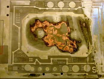
Early attempts at aluminum trace circuit boards produced black, charred panels which resembled a poorly executed wood-burning kit project of the seventies. The first visually appealing samples featured a 0.020” pitch and resulted in line reductions of between 0.002” and 0.005”.
 |
| An early Al-PCB experiment |
Advances in Al-PCBs often came as the result of an inadvertent error. For example, early in the development, we would pause the process after each step and closely examine every feature of the test piece. By the end of the process, we often were missing whole traces, hidden in the mass of tortured metal.
We were running late one night and pushed a sample through the processes in rapid succession. The result was astonishing and it was our first breakthrough. We have since determined which steps must be accelerated, which require longer takt times, and which are oblivious about processing time. In another example, we mistakenly reversed the image polarity which later provided us with a key to finally unlock the challenge of producing fine line aluminum traces.
Like all good science, our successes came from a careful, methodical design of experiments which would test a range of variables combined with keeping an eye out for serendipitous discoveries.
At the time of this writing, we have developed Al-PCBs with 0.010” pitch, selective copper plating and low resistance PTH.
The current technology state of low temperature PCBs can be found within our Al-PCB design guide.
We have shipped low temperature Al-PCBs to many of the world’s most prestigious R&D facilities.
What’s next depends on our customers’ needs as they continue to drive development of Omni low temperature superconductive PCBs.

