Design Guide for Aluminum Trace PCBs
Our boards conform to IPC-A-600 Class 2
Characteristics - 2 Layer Boards
| Specifications | Plated Through Hole Version | Non Plated Through Hole Version | |
|
Aluminum thickness |
|
20µm, 22µm (lower or higher upon request) |
30µm |
| Aluminum alloy | Pure aluminum | AL 3003 H18 | |
| Base material type | 4350B - Rogers P96/P26 - Isola |
FR4 | |
| Base material thickness | .png?width=176&name=Design%209-16-2020%2014.19%20PM%20(3).png) |
As per base material type offerings from manufacturer | 0.009"- 0.031" |
| PCB final surface finish | .png?width=176&name=Design%209-16-2020%2013.16%20PM-copy2-copy%20(1).png) |
Bare Aluminum / Aluminum with selective copper |
|
| Electrical testing | If required it would need to be accounted for during layout design | ||
| Lead time | 8 weeks standard, expedite available |
3 weeks standard, expedite available |
|
| Maximum operating temperature (Estimated) |
TBD | 110° C | |
| Minimum operating temperature | Absolute zero | ||
| Trace superconducting temperature | 1.1 Kelvin | 500 milliKelvin | |
| Minimum PCB size or Minimum customer panel PCB size | 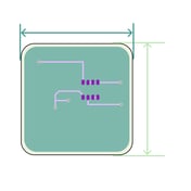  |
0.10"x 0.10" | |
| Maximum PCB size or Maximum customer panel PCB size |
|
12" x 16" | |
| PCB Panelization Options (Routing) | Singles, tab-routed, v-score | ||
| Quantity | Low to medium volume | ||
| Silk Screen |
|||
| Silkscreen colour |
|
Black or white | |
| Silkscreen layer | None, top and/or bottom | ||
| Smallest distance between silk screen lines | 0.005" | ||
| Smallest silk screen lines' width | 0.005" | ||
| Solder Mask | |||
| Solder mask colour | .png?width=176&name=Design%209-16-2020%2013.16%20PM-copy2%20(2).png) |
Green, white, black, blue or red | |
| Solder mask clearance to metal | 0.002" | ||
| Minimum clearance to unmasked aluminum | 0.005" | ||
| Smallest solder mask lines' width | 0.006" | ||
| Drills | |||
| Holes bigger than 0.250" | .png?width=179&name=Image%20from%20iOS%20(1).png) |
Are routed | |
| Intersecting or overlapping drills | .png?width=176&name=Design%209-16-2020%2013.16%20PM-copy2-copy2%20(1).png) |
Not possible, will be routed | |
| Possible drill sizes | 0.012" to 0.250" | ||
| Smallest finish hole size | 0.010" | ||
| Smallest spacing between drilled holes (drill edge to drill edge) |
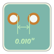 |
0.010" | |
| PTH (plated through holes) |
 |
0.012" to 0.062" | Not available |
| Available routing diameters | 0.0315" up to 0.0940" | ||
| Plated slots | .png?width=176&name=Design%209-16-2020%2013.16%20PM-copy2-copy2-copy%20(1).png) |
0.031" to 0.062" | Not available |
| Smallest radius (inner corners) |
0.01575" | ||
| Smallest routed slot width | 0.0315" | ||
| Fabrication Tolerances |
|||
| Base materials RoHS-compliance | Standard | ||
| IPC-Standards | IPC-A-600 - Class 2, if applicable | ||
| Material thickness tolerances | Dependent on base material type selected | +/-10% | |
| Max. offset drill centre to centre of reference | 0.002" | ||
| Photolithography registration tolerance | 0.005" | ||
| Routing tolerance | 0.005" | ||
| Smallest annular ring | .png?width=176&name=Design%209-16-2020%2013.16%20PM%20(2).png) |
0.005" | |
| Smallest SMD pitch | 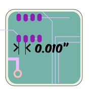 |
0.010" | |
| Smallest space width | .png?width=176&name=Design%209-16-2020%2013.16%20PM-copy3-copy%20(1).png) |
0.005" | |
| Space width variability | +/- 0.002" | ||
| Smallest trace width | .png?width=176&name=Design%209-16-2020%2013.16%20PM-copy3%20(1).png) |
0.008" (smaller upon request and at a lower yield) | |
| Trace width variability | +/- 0.002" | ||
| UL-approval | Standard | Not Standard | |
| V-Score core remaining | 0.010" | ||
| V-Score position to aluminum features | 0.015" | ||
.png?width=175&name=Design%209-16-2020%2014.19%20PM%20(2).png)
