The Superconducting Circuit Board

    What is a Superconducting Circuit Trace? How is it different from a typical Copper Trace on a PCB?


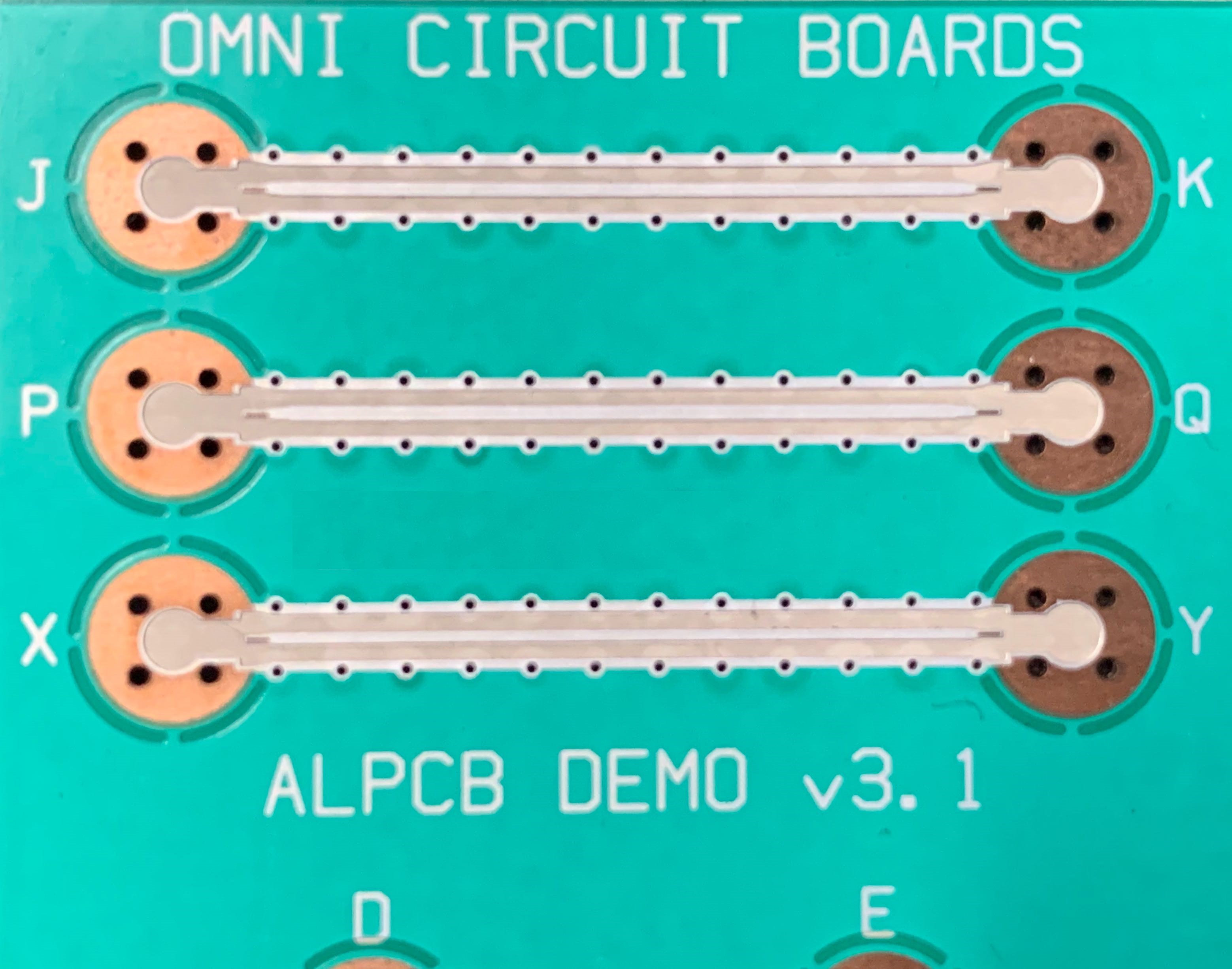
    A circuit trace is a conducting track on a printed circuit board that connects components electrically and allows electric current to flow with little resistance.

    While this small resistance is inconsequential for most applications, there are applications where the heat dissipated due to this small resistance is a big problem.

    Much like how normal conducting trace allows current to flow, they also allow heat to flow from higher temperature areas to areas of lower temperature.

    Can FR-4 PCBs be used at low cryogenic temperatures?

    What is FR-4?

    The short answer is "Yes," but there is a bit more to it.

    What exactly is FR-4? FR-4 is a NEMA grade designation for flame-resistant glass-reinforced epoxy laminate. "FR" stands for Flame Retardant. The materials used are not defined by it, so different formulations can be rated FR-4. Unfortunately, it has become the norm in the industry to refer to the most commonly used PCB material by its FR-4 designation. As different formulations can share this rating, the properties of FR-4, particularly at cryogenic temperatures, can vary significantly.

    Understanding Printed Circuit Board Manufacturing: Odd Layer PCBs

    About 8% of PCB boards we are asked to produce are comprised of an odd number of layers. But unless you have a specific signal routing requirement or need for a greater dielectric space, it is usually best to design a multilayer board with an even number of layers. Reducing an even layered board by one layer may seem like a cost-saving move, but from a Printed Circuit Board perspective it is not. It may actually increase the cost as well as lead-time and leave you with a warped PCB which may not meet your expectations. Let's look at the issues in detail.

    Understanding Printed Circuit Board Manufacturing: Avoiding File Errors

    At Omni not all PCB files we receive are from seasoned PCB design professionals.

    Designs also come to us from enterprising individuals who can credit their body of knowledge to the results of internet searches. The inspiration for this article came from one such individual.

    How to Avoid Printed Circuit Board Delays in the Quoting Process

    CAM (computer-aided manufacturing) is the art of translating a PCB board designer’s creative CAD (computer-aided design) output into information required in the manufacturing processes required to fabricate that same PCB.

    Our processes require your computer generated files to be converted into photo-tooling films and drill and router files which will allow us, the printed circuit board manufacturing facility, to produce a custom PCB to your specifications.

    Understanding Printed Circuit Board Manufacturing: Hard Gold Plating

    Plating Hard Gold onto printed circuit boards is typically done to provide contact points and PCB edge connectors.

    Gold contact surfaces are often used on circuit boards with membrane switches which are a technology of choice for industrial, commercial and consumer products. When PCBs will be repeatedly installed and removed, electroplated gold is used for edge-connector contacts or as they are more commonly known: Gold fingers. The plating thickness of a PCB gold finger is typically a mere 300 micro-inch. At this thickness the hard gold is expected to survive 1,000 cycles before wear through.

    Printed Circuit Board Design Techniques and Best Practices for Cheaper Quotes

    Using a few simple techniques can help ensure a more robust printed circuit board design which can also help you save money.

    Printed circuit board design is a balance between functionality, longevity, aesthetics and board costs, time to design and the PCB fabricators capabilities. Listed below are eleven of the most common best practices we recommend to our customers.

    Understanding Printed Circuit Board Manufacturing: Impedance Control

    Printed circuit boards with impedance requirements demand a high level of precision.

    For standard circuit boards, a PCB manufacturer is given a set of patterns - copper patterns, hole patterns, ink patterns, which are combined into a single circuit board with all the pattern sizes and positions within certain tolerances. Failure to meet a certain size or position with the specified tolerance can be cause for the circuit board to be rejected. If a trace has been defined as an impedance control trace, it is not the trace size which is strictly defined, but rather the impedance. While a nominal trace size will be provided in the Gerber layer, it is understood the circuit board manufacturer can vary trace width, height, and dielectric thickness as long as the final impedance is within tolerance.

    How Copper Weight Impacts Printed Circuit Board Manufacturing - Copper Thickness Calculator

    One of the critical steps when ordering a printed circuit board is specifying the copper weight.

    The default, should you choose not to specify a weight, is 1.2 oz of copper. This is because customers routinely specify a minimum 1 oz copper thickness and 1 mil of copper in plated through holes. To achieve this, we routinely plate up 0.5 oz base material with 0.7 oz of additional copper which provides the requested thickness in the hole. Often our PCB board quotes will reflect this specifying 0.5 + 0.7 oz Cu/sq ft where the 0.5 is the base copper and the 0.7 is the plated copper.

    Custom Printed Circuit Board Shapes

    In business as in life, we learn more from listening than talking.

    The other day we received a fairly odd question from an electrical engineer with a product development company we have worked with for many years.

    “Can you do round circuit boards?” he asked.
    “Yes…” we replied tentatively, thinking there must be so much more to the question.
    “So a board that’s three inches round… no problem?” he inquired.
    “Absolutely,” we confirmed.

    But then we began to think. If a long-time customer doesn’t know we have the capability to produce boards which aren’t just rectangular, how would a new customer know?