Avoid these four circuit board design mistakes:
1. Stipulating a "minus" tolerance on small micro via holes
2. Having Non-functional pads on inner layers
3. Not defining nor considering edge tolerances
4. Stipulating wrong copper thicknesses
1. Stipulating a "minus" tolerance on small micro via holes
2. Having Non-functional pads on inner layers
3. Not defining nor considering edge tolerances
4. Stipulating wrong copper thicknesses
%20microwave%20laminate.png)
When beginning work with a new material, you try to do as much research and get as much advice as possible.
You download the manufacturers documentation and talk with the manufacturers representatives, drill/router bit manufacturers and other PCB manufacturers who have worked on the material in the past.
After compiling all this information, a manufacturing process is developed which fits both the material and your own facility.
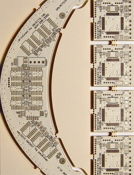
PCB Manufacturer = The company that manufactures blank PCBs for you, Omni Circuit Boards Ltd is a "PCB Manufacturer"
PCBA Manufacturer = The company that manufactures an assembled or populated PCB for you, also known as CMs or contract manufacturers.