The Superconducting Circuit Board

    Understanding Printed Circuit Board Manufacturing: Hard Gold Plating

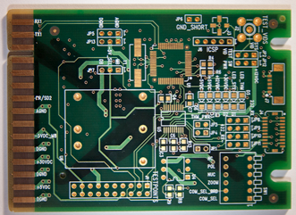
    Plating Hard Gold onto printed circuit boards is typically done to provide contact points and PCB edge connectors.

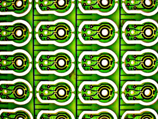
    Gold contact surfaces are often used on circuit boards with membrane switches which are a technology of choice for industrial, commercial and consumer products. When PCBs will be repeatedly installed and removed, electroplated gold is used for edge-connector contacts or as they are more commonly known: Gold fingers. The plating thickness of a PCB gold finger is typically a mere 300 micro-inch. At this thickness the hard gold is expected to survive 1,000 cycles before wear through.

    How to Get a Low Cost Printed Circuit Board Quote

    We would like to offer you step by step instructions on how to get a PCB Quote.

    First the legal requirements: quotes form an integral part of the traditional, legal, offer and acceptance contract process.

    When you receive your quote, it is your responsibility to review the specifications provided.


    4 Tips for Saving on Printed Circuit Board Prototyping Costs

    1) Not considering sufficient Thermal and antipad (solder mask) clearances

    You need to consider thermals and antipad (solder mask) clearances on the power &/or ground plane layers of multilayer boards during design. If layer to layer registration, tolerances for hole size, location, film expansion and registration have not been taken into account then manufacturing will experience high reject rates and increased costs.