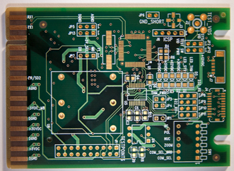
1) Not considering sufficient Thermal and antipad (solder mask) clearances
You need to consider thermals and antipad (solder mask) clearances on the power &/or ground plane layers of multilayer boards during design. If layer to layer registration, tolerances for hole size, location, film expansion and registration have not been taken into account then manufacturing will experience high reject rates and increased costs.
Antipads (solder mask clearance) should be 0.010" to 0.020" larger than outer layer pads. For thermal pads the most should be a minimum of 0.012" ( preferable 0.015") and pads should be equal to or larger than outer layer pads.
Clearances for solder masks around non plated holes should be at least 0.005"
2) Having restrictive tolerances for multilayer board thicknesses
Specifying tolerances that are very tight can result in higher costs, increased time and lower yields. It is suggested to call for restrictive tolerances only when they are critical to your design.
3) Minimum Text Widths that are Less than 0.0080” on Silkscreen Layers
Providing artwork which requires Text Widths less than 0.0080” requires extra imaging and processing steps which will increase the cost of your project.
4) Specifying hole sizes that are Less than 0.016” if not required
Hole sizes smaller than 0.016" requires PCBs to be subjected to additional chemical processing to ensure sizing and clean-outs are complete. These additional steps could add one full day to your processing time along with the associated costs.

