 The purpose of panelization is to secure PCB boards during manufacturing, shipping and assembly processes and faster throughput while making their separation as painless as possible.
PCB Manufacturer = The company that manufactures blank PCBs for you, Omni Circuit Boards Ltd is a "PCB Manufacturer"
PCBA Manufacturer = The company that manufactures an assembled or populated PCB for you, also known as CMs or contract manufacturers.
A "PCB Shop Fabrication Panel" is not the same as a "Customer PCB Panel", yet both are known as "Panels" in their respective industries.
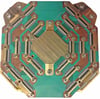
The "PCB Shop Fabrication Panel", is the panel that a PCB manufacturer like OMNI uses to fabricate your boards and panels, it usually contains several "customer PCB panels" and/or it may contain "loose" customer PCBs, also referred to as "single pcbs".
A "Customer PCB Panel", or simply a "PCB Panel" is the panel that is utilized by a Contract Manufacturer (CM) for PCB assembly, meaning, populating a PCB with SMD or PTH components and thus creating a "PCBA" ("A" stands for Assembly).
The companies that can help you panelize your single PCB design are the "PCB Manufacturers" not the "PCBA Manufacturers" because even them will outsource the panelization to a "PCB Manufacturer" like Omni.
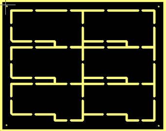
Panelization can be as simple as a rectangular board tab routed with a 100mil (0.100”) space between PCB boards and a 500mil (0.50”) border on four edges. Or, it can be as complex as a panel filled with combination of Jump V-score or routed rounded polygons.
Some guidelines for panelization are simple, for example, with routed panels:
- If the PCB is rectangular and all sides have a length greater than 1.00”, add 100 mil between PCBs and a 400 mil border along the outside.
- If all sides do not have a length greater than 1.00”, add 300 mil between PCBs and a 400 mil border along the outside.
But:
- If the PCB is not rectangular provide a 300 mil space between PCBs
- For V-Scoring use a 20mil space between the PCB board edge and copper pads or traces. Additionally, provide a 300 mil wide frame on at least two opposing sides.
As with all technical subjects, exceptions abound. For example:
- If a mounted component extends beyond the boundaries of the PCB board, the border between PCBs needs to include the overhang distance. This ensures the component is not damaged during de-panelization and doesn’t interfere with neighboring components on adjacent PCBs.
- If a particularly heavy component is to be installed, extra material will be required between PCB boards to ensure the mechanical strength of the panel.
It’s important to ensure the clearance between any metal and the edge of the PCB board is a minimum of 5mil for routing and 20mil for v-scoring.
Having the metal exposed during routing or v-scoring could lead to shorts after assembly and jagged edges.
The size and shape of the board will determine how many breakout tabs to use. Too few and the PCB may not be mechanically stable enough for assembly. Too many and the de-panelization process becomes onerous.
It is not uncommon to order a pair of boards (different designs) as a single set (customer panel PCB). So panelizing them together makes sense. This is possible with some restrictions:
- boards should be of similar size to panel efficiently.
- most board parameters must be the same.
- copper distribution needs to be similar or failures from the etching process can occur and panel will warp during reflow oven.
When panelizing for production quantities, we are often requested to provide panelization or paste files. These outputs from the CAM process enable our customers to purchase their solder paste stencils.
As manufacturers, we are faced with constant panelizing challenges.
Consider a customer who historically purchases 32 boards per order which are produced on 8 boards per panel, increasing their order quantity to 500 boards. The choice has to be made whether to produce the boards on the original panel and suffer the material waste due to poor utilization or re-panelize and produce all new tooling configurations and larger panel sizes which could in turn create warping problems while populating the PCBs.
One answer to ever changing order quantities is to adopt lean-manufacturing processes. By combining like designs on the same panels, we have been able to increase the utilization by as much as 50% and have also resulted in lead-time reductions of 20% which translates to lower price quotes.
More planning and work is required on the front end but the impact to materials and PCB manufacturing is substantial. Streamlining processes not only impacts the cost, it also helps ensure a short production window.