At Omni not all PCB files we receive are from seasoned PCB design professionals.
Designs also come to us from enterprising individuals who can credit their body of knowledge to the results of internet searches. The inspiration for this article came from one such individual.
While the internet can be a terrific resource, sometimes industry jargon can make it difficult in the beginning to move design ideas into physical reality. The process of manufacturing a PCB may be complicated but the ordering phase shouldn’t be. With this in mind, we put together this basic list.
Delays occur when designs can’t move past the quoting phase due to required design reviews that incur in back-and-forth e-mails. These delays are usually caused by only a few sources.
We offer you this half dozen simple gotchas to avoid.
- Drilling: Are the drill files and tool lists included and have you specified smaller hole sizes than really required? Nothing will stop a project in its tracks faster than not providing the drill files. Using a minimum hole size of 0.016” will help ensure your project is eligible for prototyping programs.
- Silkscreen: Are the top and bottom silkscreen files populated and included? PCB fabricators routinely receive file-sets where the bottom overlay (silkscreen) file is empty. So having an empty file won’t send up a warning flag.
- Outline: Is the mechanical/outline included? Without the extents of the design, you won’t be able to receive an accurate quote much less have production start on it.

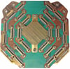
- Copper / Silkscreen combos: While designers will incorporate company names and part numbers into their copper layers, an increasing number of designs are arriving with silkscreen layers superimposed onto the copper layers. An example of this predicament is shown on the top copper layer in this image.
- Revision Control: If you submit files to your PCB fabricator and later send updated files, use and update the revision level. A challenge for even experienced designers, revision control errors can prove costly.
- Documentation: A simple way to help communicate your intent is to provide a Copper Readme or Aluminum-Trace Readme file which contains information critical to your design. Too often what seems clear to the designer doesn’t translate completely in the Gerber and drill files and features can be misinterpreted. A line may be the centerline for a routed slot or it could simply be an artifact left from an earlier design attempt.
How can these design errors be avoided?
The simplest answer is to download a viewer and review the Gerber and NC drill files before sending them to the PCB fabricator. At the very least, the communication between you and your PCB fabricator will be improved as you will both be looking at the same features.
If you have a PCB project and appreciate a friendly team to work with, please contact us.