To begin, the laminate manufacturer freely admits the material will move, but only during the etching process.
%20microwave%20laminate.png?width=335&name=Rogers%205880%20(Duroid)%20microwave%20laminate.png)
The key they state is to first etch 80% of the copper, cure the material in an oven, then provide a final etch and a final baking cure.
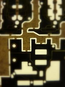
(Image by Jeff Keizer)
When beginning work with a new material, you try to do as much research and get as much advice as possible.
You download the manufacturers documentation and talk with the manufacturers representatives, drill/router bit manufacturers and other PCB manufacturers who have worked on the material in the past.
After compiling all this information, a manufacturing process is developed which fits both the material and your own facility.
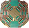
Normally these precautions are enough to ensure success but one material, Duroid, requires significantly more attention.
To begin, the laminate manufacturer freely admits the material will move, but only during the etching process. The key they state is to first etch 80% of the copper, cure the material in an oven, then provide a final etch and a final baking cure. So two films will be required for etching instead of one and it will require extra time in the ovens. Easy, right?
The panels look normal and with almost 3 decades of PCB manufacturing experience to back you up, what could go wrong?
The panels go in for first drill followed by imaging and you know immediately the process is starting to go sideways. After inspection, you determine the panel has shrunk by 0.012” over a length of 18”. To convert this into a PCB manufacturing perspective, you’re in the ditch already and you haven’t even rolled into the etching department.
All the prepared films and files are discarded and remade to compensate for the new shape and the panels go into etching where they shrink a further 0.008” but the aspect ratio is also off.
The panel isn’t shrinking in all directions at the same rate, the traces are not etching at the same rate either. In fact, each half of the panel will require two separate drill files. It’s a wreck with a lot of time and expensive material to write off.
Determined to learn all you can, the panels go in for final drill/rout. The CNC equipment feed and speeds are reduced to the provided specifications. These equipment adjustments along with double fluted end mill bits (in place of standard chip breaker bits) and dedicated holders are all recommended to help prevent costly rework labour time at the end of the process. However, the random strand feature ensures ragged edges are inevitable. You can feel momentum slowing as the final suggestion from the tooling representative is to clean it up by hand.
We have learned that each design with Duroid laminates requires at least one sacrifice production panel pcb and you can’t count on subsequent panels to behave in precisely the same manner.