CAM (computer-aided manufacturing) is the art of translating a PCB board designer’s creative CAD (computer-aided design) output into information required in the manufacturing processes required to fabricate that same PCB.
 Our processes require your computer generated files to be converted into photo-tooling films and drill and router files which will allow us, the printed circuit board manufacturing facility, to produce a custom PCB to your specifications.
Our challenge is we rarely know your design intent and in PCB manufacturing, as in life, Murphys Law applies.
Your CAD data must completely and unambiguously specify the PCB you want; otherwise, we will make something else.
Being human, mistakes happen. We would prefer not to multiply your one CAD mistake dozens or hundreds of times as real but unusable PCBs.
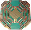
We hope you find this basic and downloadable "PCB Design Checklist" will save you time.
(Click the "PCB Design Checklist" image to download)

- Gerber files (we do receive orders missing these)
- Aperture data preferably embedded within extended Gerber format files (RS274X) which provides the shape and the size for all of the features within the printed circuit board.
- Drilling: Both the NC drill files which provide the physical location of the holes and the Drill Tool List which provides the tool sizes. The information may be separated or combined into one file.
- Mechanical layer which provides the outside profile and dimensions of your PCB board. (Please give us clean unambiguous outlines, do not forget joining line segments together to form corners)
Design Checks:
- Avoid cut metal at routed or v-scored edge
- Avoid overlapping drill locations; they cause broken drill bits
- Avoid over-tolerancing, specifically on:
- Space and Copper Trace widths
- Annular ring sizes
- Drill sizes
Documentation:
- Readme file should contain information about:
| - Cutouts | - Board thickness | - Panelization Requirements |
| - Plated/non-plated through holes | - Dielectric Material | - Solder mask color |
| - Max radii of inside routed corners | - Finished Cu weights | - Silkscreen color |
| - Surface finishes | - Finished hole sizes | - Any special requirements |
An example of a "Copper PCB Readme file" or an "Aluminum-Trace PCB Readme file" can be found downloading the respective link.
- Avoid part number and revision discrepancies. Any discrepancy between the part number or revision on the order, file names or physically on the circuit board will bring the process to a grinding halt.
- Inner layers of Multi-layer designs need to have the layer order specified and each layer must be unambiguously identified.
It may help to think of the CAM department in a PCB shop as the gatekeeper to manufacturing.
No design hits the shop floor until it meets with the approval from the customer. Checking these basic points will ensure your PCB board quote and order are not delayed
Are your files ready? Send them to us for a quote