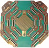
One of the more artistic processes in a PCB manufacturing facility is the application of Silkscreen known in the old days as Ident layers.
Silkscreen is usually white and human readable letters, normally used to identify components, test points, PCB and PCBA part numbers, warning symbols, company logos, date codes and manufacturer marks.
Silk-screening requires specially formulated inks. The standard colour is white, but you can also select red, blue, black, yellow, etc.
At one time, PCB CAD software allowed for a few standard fonts to be used in silkscreen layers. Now, many packages allow for all available system fonts to be used. Be careful when choosing your font. It may seem interesting to pick a “Gothic” font but remember someone needs to read it later specifically, the people assembling your boards, quality inspectors, etc.
PCB manufacturers are required by IPC to provide both a manufacturer’s mark and an identifier which will allow for lot tracing should problems occur. Although there are no strict standards for where these markings appear, manufacturers will generally try to place them in non-critical areas. But just because you know the board will also double as a backlit equipment faceplate with your company logo doesn’t mean your PCB manufacturer will. If you require these markings to be placed in a specific area or omitted, you need to specify it in the "Copper PCB Readme File" or the "Aluminum-Trace PCB Readme File", in a fabrication drawing or in your communications with the manufacturer.
Omni Circuit Boards Prototyping Services all come standard with green solder mask and white silkscreen on both PCB sides. We do have a minimum size of 8 mil (0.008”) line width for all lettering and graphics. If you have a requirement for Prototype Services we invite you to put us to the test.
Screen-printing is done when the boards are still panelized prior to the application of the final finish or routing/v-scoring.
Conventional silk-screening requires polyester screens stretched across aluminum frames. Solvent resistant emulsions are used to coat the screens prior to imaging. Both the screen and panel must be registered precisely to ensure proper alignment. This method of screening requires the following equipment: Laser photo plotter to produce the initial film, UV printer, spray developer and curing ovens. Screens can be cleaned and reclaimed to be used again although not for jobs which require high resolutions.
Currently three methods are available for applying the “Silk screen or Ident” to the PCB.
- Manual screen-printing can be utilized when line widths are greater than 7 mil (0.007”) and the registration tolerance is 5 mil.
- LPI (Liquid Photo Imaging) provides more accuracy and legibility than manual screening and is employed when line widths are greater than 4mil.
- DLP (Direct Legend Printing) is the most accurate and legible of the 3 processes but also has the highest cost for consumables.
The art of manual silk-screening takes time to develop. At Omni, our master craftspeople have been practicing their art for over 20 years. Some of the parameters to be considered include the viscosity of the ink, room temperature, humidity, age of the ink and hardener and line resolution.
From these variables the correct amount and distribution of ink, the stroke force and angle are derived, as they will impact the final outcome.
PCB layout designers sometimes forget to double-check their silk screen layers before sending designs to PCB fabrication. Designers should avoid putting ident over component pads, they should avoid using excessively tiny text and should allow for registration tolerances.