 About 8% of PCB boards we are asked to produce are comprised of an odd number of layers. But unless you have a specific signal routing requirement or need for a greater dielectric space, it is usually best to design a multilayer board with an even number of layers. Reducing an even layered board by one layer may seem like a cost-saving move, but from a Printed Circuit Board perspective it is not. It may actually increase the cost as well as lead-time and leave you with a warped PCB which may not meet your expectations. Let's look at the issues in detail.
Cost savings:
An odd number of layers means one layer is blank (meaning without copper), so no mylar film needs to be created by the CAM Department for that layer. This represents a small saving in the CAM department, however the processing cost while manufacturing the PCB will increase. If cost savings are the main reason you are entertaining an odd layer design, you may realize more tangible results by reviewing our article on design techniques and best practices.
Possible additional costs:
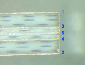
A multilayer board is manufactured by laminating multiple "2 layer boards" together into a single stack. They are pressed together at a high temperature for several hours in a special PCB press that applies pressure and heat.
Once the curing process is complete, the PCB boards are allowed to cool before being removed from the press.
To make an odd layer PCB, we normally use a standard symmetrical even layer recipe on that press and at a later stage we completely etch away one copper layer. We do it this way because this is the most reliable way to ensure the bondability of an odd layer PCB.
Different materials contract different amounts during the cool down, so asymmetrical builds will have asymmetrical stresses.
An odd number of layers means one of those "2 layer boards" becomes a "1 layer board" – meaning, it has copper traces on one side and all of its copper metal etched away from the other side. This has a few implications including added processing cost due to extra etching step and PCB warpage.
By etching away all of the copper from one side of the PCB board your panel tends to warp during the cooling stage, this occurs because you end up with two different materials on each side which cool down at different rates and this creates asymmetrical stress on the PCB.
Warpage causes several problems for production.
Limiting warpage in any multilayer PCB board requires care in ensuring a balanced stack-up of base and pre-preg layers, and this is made even more challenging with an odd number of layers. Even when warpage can be controlled in PCB production, you may find it is worse after wave or reflow soldering when populating the PCB with components.
One area of misinformation surrounding odd layer count designs is its impact on the copper etching process. Contrary to belief there is no risk of over-etching when one side is being completely etched away and the reverse design has finer elements, however having odd layer count designs become an area of concern in the copper plating process.
Having a significantly different weight of copper to plate to each side increases the risk of either under or over plating. It’s a bit like pan frying an egg in a heavy cast iron pan and expecting the top side to cook at the same rate as the pan side.
Alternatives
If there is no design reason to keep to an odd number of layers, then don't.
Use an even number of layers content in the knowledge that using one less layer doesn't help anyone. If the number of power or signal layers is odd, add another one. Ideally, you want the number of power and signal planes to be even as well.
If you have a 3 layer design, but it doesn't need to be 3 layers, the easier way to achieve copper balance is to just duplicate the inner layer.
If you decide for design reasons that you can only live with an odd number of layers, rest assured we can make it work for you.
Additional steps can be taken to try to keep your multilayer PCB board within IPC warpage specifications to meet your requirements but you may find it incurs additional cost and time.