The journey to develop a circuit board which features aluminum circuitry (Aluminum PCBs ) has been challenging.

Beginning in 2008, Omni Circuit boards was challenged by a strategic partner with developing a circuit board with fine-line aluminum traces. The reason for aluminum in the initial quest was for its superconducting (cryogenic) properties. But as time went by, we began to appreciate how developing this capability could also benefit customers who have a requirement for aluminum wire bonding of critical components and non-magnetic properties.
Initial research uncovered numerous previous attempts to etch aluminum circuit designs although we could not find evidence of successful commercialization of the process. Some information would be gleaned from expired patents, but in the end, the process required a stream of painstaking lab and field tests.
It would be 5 years before the development team could graduate from working with simple test patterns to functional circuit boards which could be populated and installed in customer products.
The development team has changed over the years, but the group that successfully found a way to commercialize these PCBs which are capable to operate at very low temperatures was mainly comprised of chemists, engineers and production personnel.
The key to this process is a micro-foil material constructed of a 40 µm core of aluminum with a 5 µm electro-deposited layer of copper. This micro-foil is then laminated onto a non-conductive substrate (typically FR4).
The process of manufacturing Aluminum Printed Circuit boards is much the same as traditional PCB production until the etching process:
- Cad / Cam work is performed from supplied customer files
- Film is produced on a photo plotter
- The Al / Cu foil is laminated onto a non-conductive substrate
- A photo-resist is applied to the circuit board
- The circuit is imaged onto the laminated board
- A series of aluminum and copper etches are conducted before a final copper etch to remove unwanted copper
- Mechanical drilling and routing is done before and/or after etching
- Solder mask and/or Component Silkscreen are applied in the conventional manner
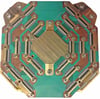
The result is a lightweight bi-metal electronic circuit board with fine-line aluminum conductors.