PCB manufacturing facilities routinely perform Electrical Testing with “Flying Probe” testers which are well suited to smaller production runs.
For short runs, the flexibility of quick set-up ensures cost effective Flying Probe tests outperform the lead-time, cost and fixed designs of dedicated test beds.
With Flying Probe tests, no fixtures need to be prepared, only data files.
Flying Probe tests are able to reveal not only shorts and opens produced by the manufacturing process but have also been known to expose design errors.
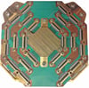
Flying probe tests utilize several test heads, each equipped with a precision probe which moves to test points, vias, component pads and circuit interconnects on both surfaces of the PCB at very high speeds.
Boards are first probed to search for “opens”, i.e. broken traces or inadequately plated holes. Then a second pass looks for short circuits “shorts” between nets. These probes are controlled by XYZ servo-systems and can contact pads only a few mils (thousandths of an inch) across and a few mils apart.
Providing circuit board designs with dedicated test points adds time and cost at the PCB level. Test points at the ends of all nets, traces and edge connectors enhance testability of PCBAs but each of these points must also be tested by the flying probe.
The trade off is easily in favour of PCBAs, where the cost of the circuit board ramps up. For high value and very complex circuit boards, we will typically conduct two ICT tests, one before solder masking and one after final routing.
Flying probe testing utilizes proprietary software to evaluate the circuit board Gerber (CAD) files to generate an X-Y Netlist. It then analyzes the Netlist utilizing a sequential path logic to ensure high fault coverage of nets (i.e. trace patterns).
Electrical Testing is highly recommended for multi-layer PCBs as well as boards which will be populated with high value components.
In addition, PCB designs with copper “poured” to cover most of the board surface surrounding pads and traces are more likely to have short circuits and are more likely to benefit from electrical testing.
Typically, the cost of the test represents a very small percentage of the finished board cost which can yield a large payback.