Avoid these four circuit board design mistakes:

1. Stipulating a "minus" tolerance on small micro via holes
2. Having Non-functional pads on inner layers
3. Not defining nor considering edge tolerances
4. Stipulating wrong copper thicknesses
1) Stipulating a "minus" tolerance on small (micro) via holes
This might cause limitations on panel size due to pad/hole ratios.
High current densities might plate the hole down. Reworking the vias to unplug the holes is time consuming.
Specify if vias can be filled or designate tolerances as a "+" allowance only or specify that vias may be plugged or filled
2) Having Non-functional pads on inner layers
Routing traces too close to plated through holes.
In designing a board "minimum spacing" is an important consideration.
Often, this spacing does not take into account manufacturing tolerance buildup (i.e. maximum allowable mis-registration combined with maximum etch back).
A trace routed between plated through holes on a layer with the nonfunctional pads removed can actually short out during an electrical test resulting in a scrapped unit.
If pads do have to be removed (as is the case in flex or rigid/flex boards) it is advisable to let the manufacturer take care of this.
3) Not Defining nor Considering Edge Tolerances
Ground planes (and traces) should end approx. 0.010" from the edges of the board to ensure against accidental shorting with metal chassis and cases.
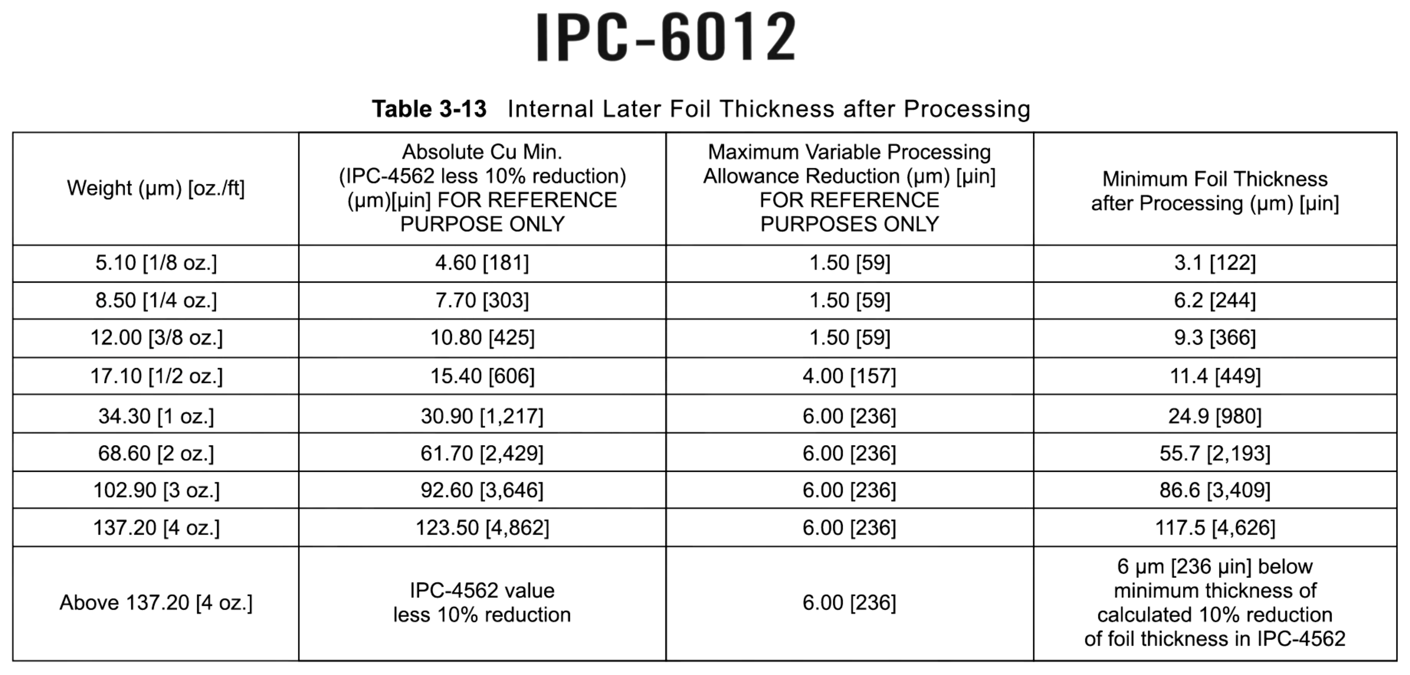
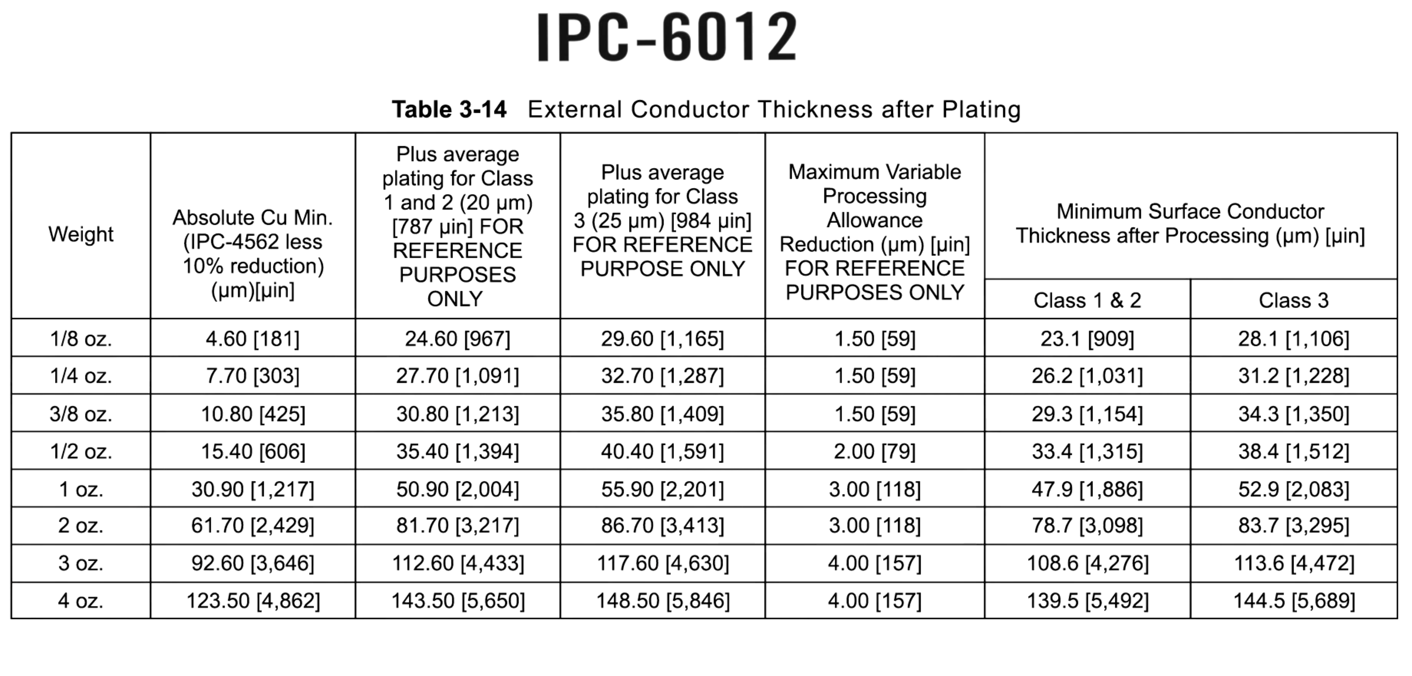
4) Stipulating Wrong Copper Thicknesses
- Finish Thickness Copper = After plating (External Conductor Thickness After Plating)
- Base Thickness Copper = Before plating (Copper Foil Thickness After Processing)
- Ounces = Weight of copper that covers 1 square foot
Often designers request 1 ounce of copper as a finished thickness whether they intend for a finished copper thickness of that dimension or not, this means we then need to start with a base copper foil thickness of 2 ounces which after processing will provide us the expected 1 ounce finished copper. Having to start with a 2oz copper foil significantly increases your quote pricing.
Being specific as to the parameters that you require will ensure that your design will not fail and that your quote is on point.
You can find more information on this regard under IPC-6012D: Qualification and Performance Specification for Rigid Printed Boards